Here is something most engineering students in India do not know: the government is giving away access to professional chip-design software that costs tens of thousands of dollars per licence commercially — for free — to enrolled engineering colleges. And Chandigarh is one of only four national training hubs for the programme.
The programme is called Chips to Startup, or C2S. If you are an ECE student, a faculty member, or someone with a college-going child in an engineering programme, this is worth understanding.
What C2S actually is
Chips to Startup (C2S) is a programme run by the Ministry of Electronics and IT (MeitY) under the India Semiconductor Mission. Its purpose is simple and ambitious: put the same chip-design tools used by Intel, Qualcomm, and Nvidia into the hands of Indian students and faculty, so that India builds a domestic pipeline of semiconductor design talent.
The scale so far:
- 315+ institutions already enrolled, with a target of 500 under the next phase of the Semiconductor Mission
- 85,000 chip-design engineers targeted for training
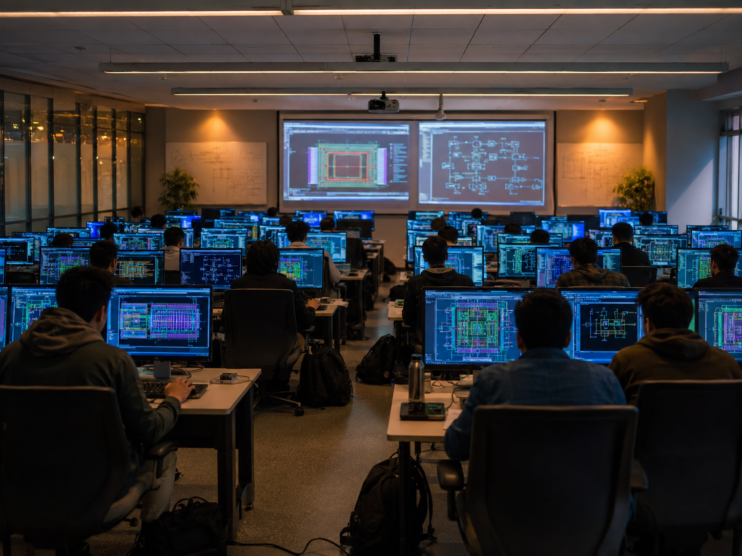
- Free access to the full professional toolchain from Synopsys, Cadence, and Siemens — the three EDA (Electronic Design Automation) vendors that power chip design at every major semiconductor company in the world
- Launched in 2021 alongside the first phase of the India Semiconductor Mission
These are not student versions or trial licences. They are the actual industry tools — Synopsys Design Compiler, Cadence Virtuoso, Siemens Calibre, and more — the same software a design engineer at a chip company uses every day.
The Chandigarh connection
Here is why this matters specifically for the ISTCKonnect region.
Once a college is approved for C2S, its faculty must undergo mandatory training before they can access the tools. This training is delivered at NITTTR — the National Institute of Technical Teachers Training and Research — and there are only four NITTTR centres in the country that run it: Bhopal, Chennai, Kolkata, and Chandigarh.
NITTTR Chandigarh, located in Sector 26, is therefore one of the national nodes through which India's semiconductor design faculty are being trained. For engineering colleges across Punjab, Haryana, Himachal, and the wider North Indian region, the C2S faculty training pathway runs through Chandigarh. The tricity is not on the periphery of India's semiconductor push — on the design-talent side, it is one of the training centres of it.
Who can benefit
C2S is aimed at AICTE-affiliated engineering colleges with ECE, EEE, or CSE departments, and at NAAC-accredited degree-granting institutions. The institution needs to commit dedicated VLSI-lab space and have at least one faculty member with a semiconductor-design background.
For students, the benefit is direct: if your college is enrolled in C2S, you get to learn on the actual tools used in the industry during your 3rd and 4th year, use them for your final-year project, and — for top performers — access semiconductor-design bootcamps and NSDC-certified programmes. Some enrolled institutions have used C2S outcomes as placement hooks with fabless design companies in Bengaluru, Hyderabad, and Pune.
One important thing to understand — design is not manufacturing
C2S is a chip design programme. It trains students for roles at fabless companies — Qualcomm India, Nvidia India, MediaTek, and system-design firms like Tata Elxsi and L&T Technology.
It does not train students for the manufacturing side of the semiconductor industry — the OSAT and ATMP facilities like Micron in Sanand, Kaynes Semicon, and Tata's assembly and test units that are being built across India right now. Those facilities need equipment engineers, process technicians, and hands-on manufacturing skills — exactly the kind of precision-engineering profile that institutes like ISTC produce, and that no EDA tool teaches.
This distinction matters. India's semiconductor story has two halves — design and manufacturing — and they require completely different training. C2S serves the design half well. The manufacturing half is where the more acute talent shortage sits today, and where a precision-engineering background becomes a strategic advantage.
The full picture
C2S is one piece of a much larger semiconductor build-out happening across India — the fabs, the OSAT facilities, the equipment ecosystem, and the talent programmes underpinning all of it. For a detailed breakdown of the C2S programme — the complete list of free EDA tools, the step-by-step application process for institutions, VLSI-lab setup requirements, and how C2S fits into the broader design-versus-manufacturing talent picture — this in-depth guide covers it thoroughly:
Why ISTCians should care
The semiconductor industry is one of the most significant industrial opportunities of this decade for Indian engineers. Whether the entry point is chip design (through C2S and an ECE pathway) or semiconductor manufacturing (through precision engineering and OSAT skills), the demand for trained people over the next five years will be substantial.
For the ISTCian community — spanning precision engineering, electronics, mechatronics, and automation — the manufacturing side is the natural fit. But understanding the whole landscape, including the design side that C2S powers, is part of being positioned well for what is coming.
Chandigarh is already on this map. The question worth asking is how much of the opportunity the region's students and institutions choose to capture.
👉 ISTCians and the semiconductor moment — why precision manufacturing is the skill India cannot import
👉 NITTTR Chandigarh admissions — B.Tech, M.Tech, and PG diploma for working professionals
C2S is a MeitY programme under the India Semiconductor Mission. Official information: chips2startup.meity.gov.in. This article is for the information of the ISTCKonnect community.