ISTCians have always worked at the intersection of machines and precision. The toolmakers, the metrologists, the automation engineers, the people who understood tolerance at 0.001mm when everyone else was rounding to the nearest millimetre. That intersection now has a new name in industry: mechatronics. And the industry it is most urgently needed in right now is one that did not exist on Indian soil twelve months ago.
India is building semiconductor factories.
What is actually happening
This is not a government announcement or a feasibility study. It is a construction schedule.
Micron Technology opened its assembly and test facility in Sanand, Gujarat in early 2025. It is operational. Kaynes Semicon reached full commercial production in March 2026 — 6.3 million chips per day. CG Power and Renesas have been running a pilot OSAT line since August 2025. The Tata Electronics–PSMC fab in Dholera — India's first commercial logic fab, 28nm process nodes, 300mm wafers, Rs. 91,000 crore — is targeting first silicon before the end of 2026. ASML, the Dutch company that manufactures every EUV lithography machine on earth, signed an equipment agreement with Tata Electronics in May 2026.
In Odisha, Sancode Semi received state government approval in February 2026 for a Rs. 1,650 crore OSAT unit in Khordha district. 570 direct jobs. And closer to home: SCL Mohali, India's only government semiconductor fab, has a Rs. 4,500 crore modernisation announced in November 2025. CDIL in Mohali — India's oldest semiconductor company, 60 years old — received ISM approval for expansion in August 2025.
The semiconductor industry has arrived in India. The question for engineers in this network is what it means for them.
Where mechatronics fits in a semiconductor facility
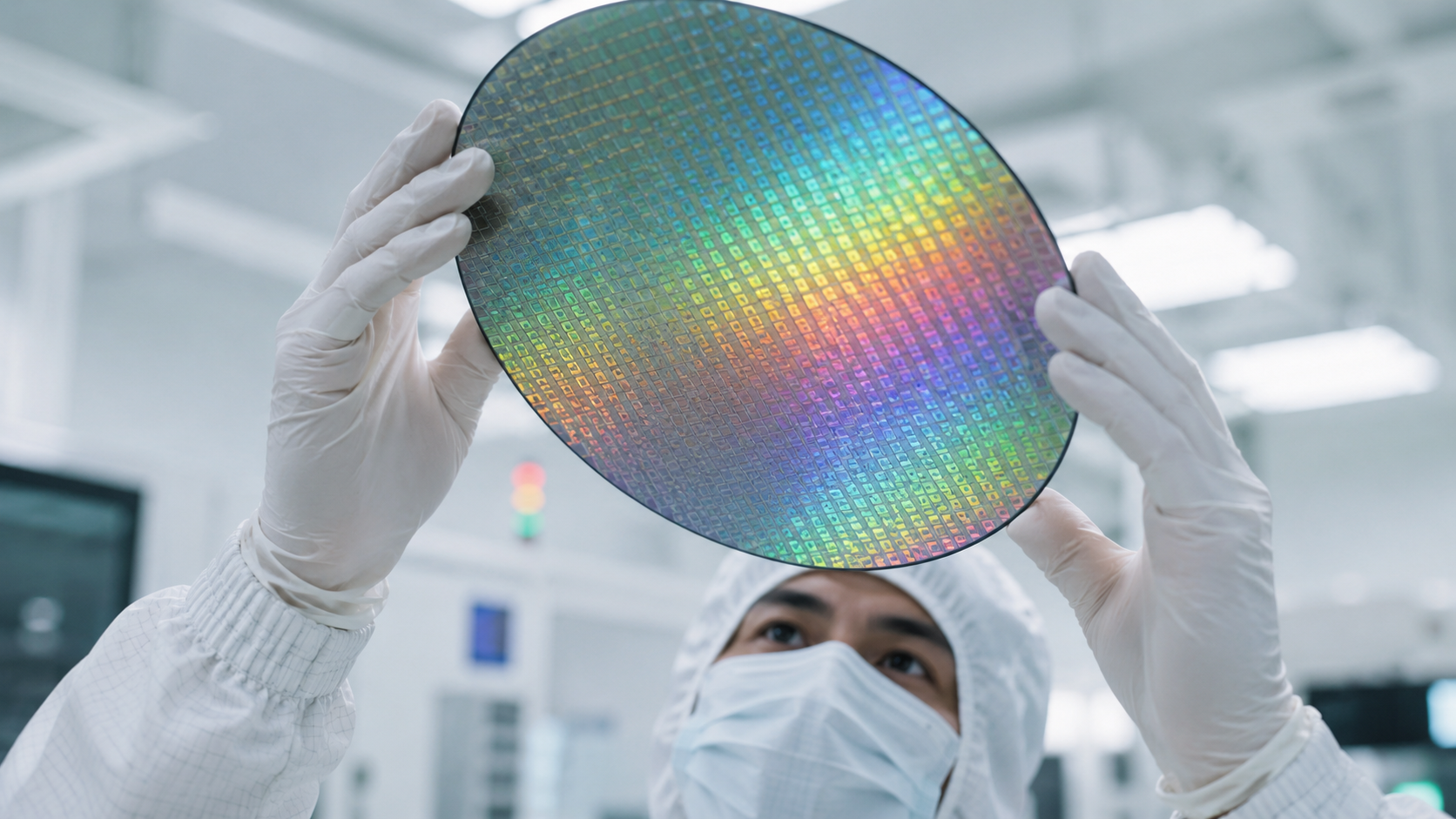
The word "semiconductor" makes most people think of chip designers — VLSI engineers, RTL coders, EDA tool users. That is the design side of the industry, and it is important. But a semiconductor fab or OSAT facility is primarily a manufacturing environment. And manufacturing environments run on mechatronics.
Every piece of equipment in an OSAT facility — die bonders, wire bonders, encapsulation moulding presses, automated test equipment, wafer dicing saws, pick-and-place robots, inspection systems — is a mechatronic system. It combines precision mechanical design, servo and motion control, pneumatics, vision systems, embedded controllers, and real-time feedback loops. Someone has to commission these systems. Someone has to maintain them, calibrate them, troubleshoot them when they drift, and qualify them when they are replaced.
That someone is an equipment engineer with a mechatronics background. In every OSAT and ATMP facility globally, equipment engineers are among the highest-demand profiles. They are also among the hardest to find — because the combination of mechanical precision, electrical systems knowledge, and process understanding that the role requires is exactly the combination that traditional engineering education struggles to produce.
ISTC produces it by default.
The ISTC skill map, read against semiconductor requirements
Consider what the ISTC curriculum actually builds and map it against what a semiconductor equipment engineer does daily:
Precision measurement and metrology. ISTC graduates can read and use a coordinate measuring machine, a surface roughness tester, an optical comparator. Semiconductor process equipment requires constant metrology — layer thickness measurement, critical dimension measurement, overlay measurement. The instruments are different (KLA, Onto Innovation, Applied Materials inspection tools instead of CMMs), but the discipline of measurement, calibration, and uncertainty quantification is identical. An ISTCian transitions to this environment faster than a general ECE graduate does.
Machine setup, alignment, and qualification. Setting up a jig boring machine or a surface grinder to tolerance requires understanding of machine geometry, thermal compensation, and systematic error sources. Setting up an ASML DUV scanner or a CVD deposition tool requires the same understanding at a different scale and in a controlled atmosphere. The qualification methodology — baseline, process window, repeatability, reproducibility — is the same discipline.
Automation and motion control. ISTC's automation and CNC training gives graduates a working model of how a controlled machine responds to commands, where errors accumulate, and how to diagnose systematic vs. random failure. A semiconductor fab's automated material handling system — the AMHS that moves cassettes of wafers between tools — is a large-scale automation problem. The wafer handler inside each tool is a small-scale one. ISTCians with CNC and automation backgrounds have the mental model to work with both.
Hydraulics, pneumatics, and mechanical systems. Semiconductor equipment is full of pneumatic actuators, vacuum systems, and fluid delivery systems for process chemicals. An ISTC-trained toolmaker who understands hydraulic circuits and pneumatic logic has a direct skill transfer into the equipment engineering role at an OSAT facility. These are not adjacent skills. They are the same skills applied in a different environment.
Quality systems and SOP discipline. ISTC's manufacturing environment runs on SOPs, inspection protocols, and quality records. Semiconductor cleanrooms run on the same logic, at higher stakes. An engineer who has spent three years working in an environment where a deviation from procedure has real consequences transitions to the cleanroom culture faster than someone who has not.
The roles that are opening
For ISTCians considering what this industry means for their careers — whether they are five years in or twenty-five — the relevant roles are these:
Equipment engineer. Owns one or more tools in the fab or OSAT line. Responsible for uptime, qualification, calibration, and escalation. The role that most directly maps to an ISTCian's background. Entry-level at 2–5 years of experience, typically paying Rs. 6–14 LPA at Indian facilities with room to grow significantly as the industry scales.
Process technician / senior technician. Runs individual process steps, monitors process parameters, identifies drift early, escalates systematic issues. A diploma-level entry point at many OSAT facilities, with a clear progression to process engineer. ISTC's 3-year training programme places graduates above this entry level on day one.
Maintenance engineer. Preventive and corrective maintenance of fab equipment. Deep mechanical and electrical systems knowledge required. An ISTCian with tool maintenance experience is overqualified for the maintenance technician role and appropriately qualified for the maintenance engineer role.
Automation / robotics engineer. As semiconductor facilities in India mature, automation of material handling, inspection, and test becomes a priority. Engineers who can design, commission, and maintain robotic systems for semiconductor environments are already scarce globally. In India, they essentially do not exist yet. An ISTCian with robotics and automation training who adds semiconductor domain knowledge early is positioning themselves for a role that will be in high demand within five years.
Vendor / field service engineer for semiconductor equipment companies. ASML, Applied Materials, Lam Research, KLA, Onto Innovation, Advantest — every major semiconductor equipment company will need field service engineers in India as the fabs and OSAT facilities come online. These are the engineers who install, commission, and service the equipment. Pay is typically higher than in-fab roles. The skill requirement is mechatronics plus domain knowledge of specific tool platforms. ISTCians who get in early — through internships, through technical training, through direct application to equipment company India offices — will have an advantage that only narrows as more engineers enter the space.
What "getting in early" looks like
The semiconductor facilities that are operational or under construction in India right now — Micron Sanand, Kaynes Semicon Sanand, CG Semi Sanand, Tata TSAT Jagiroad, SCL Mohali — are hiring. Not in large numbers yet. But the engineers who join in the first two or three years of a facility's life build institutional knowledge that is impossible to replicate later. They become the senior engineers and team leads when the facility scales. They are the ones who train the next cohort.
For ISTCians currently in automotive, aerospace, defence, or industrial manufacturing who are thinking about a sector change — the transition to semiconductor equipment engineering is lateral in skill terms and upward in trajectory terms. The domain knowledge gap is real but learnable. The precision manufacturing foundation is not teachable in a short course.
For current ISTC students and recent graduates — the question is not whether semiconductor is a good career path. It is whether you want to be among the first hundred Indian engineers with combined ISTC-level precision manufacturing training and semiconductor domain experience, or among the ten thousandth.
The first hundred will not have to prove their value. The ten thousandth will have to compete for it.
SCL and CDIL — the local angle
For ISTCians in the Chandigarh–Mohali–Tricity corridor specifically: SCL Mohali is 15 minutes from ISTC. It is India's only operating government semiconductor fab. Its Rs. 4,500 crore modernisation will require engineers who understand precision manufacturing in a controlled environment. CDIL's ISM-approved expansion in Mohali will create new production engineering and equipment roles. These are not distant opportunities in Gujarat. They are local.
The ISTC–SCL connection is not a new idea. The Indo Swiss Training Centre was founded precisely to build the kind of precision manufacturing talent that high-technology facilities need. SCL was founded to be exactly that facility. The two institutions have coexisted in the same city for over 40 years. The current semiconductor moment is the first time in a generation when the connection between them has direct commercial relevance at scale.
If you are an ISTCian and you have been waiting for a moment when your specific combination of skills — precision, metrology, systems thinking, manufacturing discipline — becomes a strategic advantage in a high-growth industry rather than a niche credential in a slow-moving one: this is that moment.
The fabs are being built. The equipment is being installed. The engineers who understand how machines actually work — not in simulation, not in theory, but in metal and tolerance and calibration — are the ones who will run them.
ISTCKonnect covers engineering career developments and opportunities relevant to the ISTC alumni community. For the full picture on India's semiconductor build-out, see fidus.one/india-semiconductor-industry. For the talent gap analysis: fidus.one/semiconductor-education-india-2026.