Every few weeks, someone in the ISTC network asks a version of the same question: "I keep seeing OSAT and ATMP mentioned together — are they the same thing? Which one is India actually building?"
It's a fair question. The two terms travel together in every government announcement, every MoU signing, every semiconductor policy document — but they're rarely explained clearly. And if you're thinking about where your skills fit in India's chip ambitions, the distinction matters.
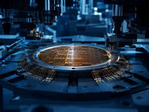
First: What India Is Actually Building
India isn't building chip fabs in the near term. Fabrication — the front-end process of printing transistors onto silicon wafers — requires decades of accumulated process knowledge, hundreds of billions in capital, and a talent pipeline that doesn't yet exist at scale.
What India is building, right now, is back-end semiconductor infrastructure: the facilities that take finished wafers and turn them into usable chips through assembly, testing, marking, and packaging. This is the OSAT/ATMP space.
The Micron plant in Sanand, the Tata Electronics facility — these are all back-end operations. The India Semiconductor Mission's approved projects to date are overwhelmingly in this category.
OSAT and ATMP: Not the Same Thing
This is where most explainers fall short. OSAT (Outsourced Semiconductor Assembly and Test) and ATMP (Assembly, Testing, Marking, and Packaging) describe overlapping but distinct concepts.
OSAT is a business model — it describes companies that provide packaging and testing services to fabless chip designers and IDMs on an outsourced basis. Think ASE Group, Amkor, JCET. They don't design chips; they finish and verify them.
ATMP is a process description — it describes the four stages of back-end semiconductor manufacturing regardless of who is doing them.
An OSAT company runs ATMP processes. But an IDM running its own back-end in-house is doing ATMP without being an OSAT.
For a clean breakdown of how the two relate — including where India-specific facilities sit in that picture — this explainer on OSAT and ATMP in semiconductors covers the distinction in depth with a practical comparison.
Why the Talent Gap Is the Actual Bottleneck
India has approved the facilities. The capital is committed. The land is allocated.
What isn't ready is the workforce. ATMP operations require engineers and technicians trained in wire bonding, flip chip assembly, advanced packaging formats (fan-out wafer-level packaging, 2.5D/3D stacking), and parametric test engineering. These are skills that weren't in mainstream Indian engineering curricula two years ago.
The India Semiconductor Mission has flagged this explicitly — the talent gap is now the critical path item. Facilities will be operational before trained people are available to run them at scale.
This is also the window. The engineers and technicians who build semiconductor-relevant skills in the next 18-24 months are the ones who will be placed in the first wave of ATMP hiring. The second wave will have competition.
If you're actively looking at what courses and programmes exist right now — from government-backed ISM skilling initiatives to private institutions that have started VLSI/packaging modules — this breakdown of semiconductor courses available in India maps the current landscape across design, manufacturing, and OSAT-specific tracks.
What This Means for the ISTC Network
ISTC has always been a bridge between institutional knowledge and industry application. The semiconductor moment is exactly the kind of structural shift where that positioning matters.
A few things worth watching:
CSIO's relevance is real. Instrumentation, precision electronics, test and measurement — these are foundational to ATMP operations. The skills in this network are closer to semiconductor manufacturing requirements than most people realise.
The component supply chain is an adjacent opportunity. India's ATMP buildout will need domestic suppliers of substrates, leadframes, EMC compounds, and precision tooling. That's an industrial ecosystem play, not just a chip play.
BD and consulting opportunities are opening. As Indian companies figure out how to position for OSAT contracts from global fabless players, there's demand for people who understand both the technical requirements and the relationship landscape.
For context on how a specialised practice in semiconductor talent enablement fits into this picture — connecting OSAT/ATMP facility operators with trained workforce pipelines — the Fidus semiconductor practice page outlines the structure of this work.
The Short Version
India's semiconductor story right now is an OSAT/ATMP story. The terminology is confusing because it's used loosely. The opportunity is real because the talent gap is real. And the window to build relevant skills before the first wave of hiring is measured in months, not years.
If this is adjacent to your work — in instrumentation, electronics, industrial R&D, or technical education — it's worth understanding clearly.
Fidus Synergies is a Mohali-based advisory firm working on semiconductor talent enablement, connecting OSAT/ATMP facility operators with trained workforce pipelines. ISTC alumni with interests in semiconductor skilling, precision manufacturing, or industrial consulting are welcome to connect.